AI
A Stealth Startup Thinks It Just Hacked the Memory Shortage
Silicon Valley startup Kepler Computing has emerged from stealth mode after seven years of developing a new architecture for high-bandwidth memory (HBM)
Key takeaways
- Kepler Computing has developed a new memory architecture that increases density without relying on EUV lithography.
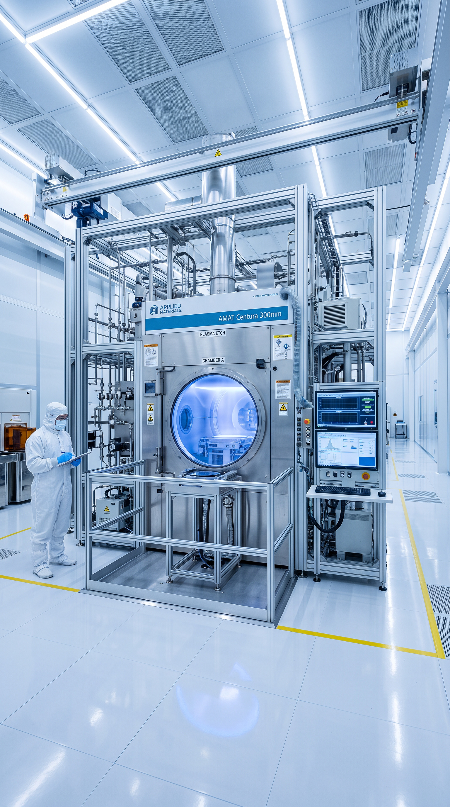
- The company can convert an existing fab into a next-generation fab in eight months instead of the typical 24 months.
- Kepler plans to ship its first samples of HBM chips later this year.
- The fundamental breakthroughs have happened, but the challenge remains in getting good results on thousands of wafers.
- The composite material contains iron, which is a contaminant that requires dedicated equipment or full encapsulation.
Silicon Valley startup Kepler Computing has emerged from stealth mode after seven years of developing a new architecture for high-bandwidth memory (HBM) and SRAM. By utilizing a proprietary ferroelectric composite material and 3D stacking, the company claims it can match the density of 2nm or 3nm chips without relying on expensive extreme ultraviolet lithography (EUV) equipment. Kepler has raised $468 million from backers including Intel Capital, AMD Ventures, and Bill Gates, alongside a $245 million commitment from the US Department of Commerce. The company plans to ship its first HBM samples later this year, ramp up production in Singapore in 2027, and begin US manufacturing in 2028.
Bypassing EUV lithography could dramatically lower the cost and time required to scale AI memory.
In their words
“Our goal is to take the fabs and architectures already built, and push them to the limits of physics.”
“Iron is a tough contaminant to introduce into a production facility. So Kepler’s solution has to run on dedicated equipment, or be fully encapsulated so that it can’t escape.”
By the numbers
- $468M
- Funding raised by Kepler over the past few years
- $245M
- US Department of Commerce commitment to Kepler
- $50M
- GlobalFoundries' investment in Kepler Computing
- 2,000
- Wafers Kepler has run its technology on
- 8 months
- Time Kepler took to convert a fab
How it unfolded
- Kepler Computing founded by physicists and computer scientists
- ChatGPT launch prompts Kepler to start HBM roadmap
- US Department of Commerce commits $245 million to Kepler
- Kepler plans to ship first HBM chip samples
Turn stories like this into views
Ravenclip finds the AI news, makes the video, and posts it before attention moves on.
Common questions
- What happened with Kepler Computing?
- Kepler Computing has developed a new memory architecture that increases density without relying on EUV lithography.
- Where can I read the original report?
- Read the full report at Wired.